7
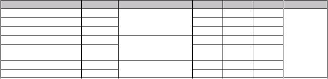
10.Timing Characteristics
Write cycle (Ta=25, VDD=5.0V)
Parameter
Symbol
Test pin
Min.
Typ.
Max.
Unit
Enable cycle time
tc
500 - -
Enable pulse width
tw
300 - -
Enable rise/fall time
tr, tf
E
--25
RS; R/W setup time
tsu1
100 - -
RS; R/W address hold
time
th1
RS; R/W
RS; R/W
10 - -
Read data output delay
tsu2
60 - -
Read data hold time
th2
DB0~DB7
10 - -
ns
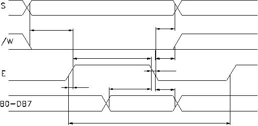
Write mode timing diagram
tc
tsu2
th2
VALID DATA
VIL1
VIH1
VIL1
VIH1
VIH1
tr
tw
tsu1
VIL1
VIL1
VIL1
VIH1
th1
VIH1
VIL1
VIL1
tf
th1
VIL1

发布紧急采购,3分钟左右您将得到回复。
相关PDF资料
NHD-0220GZ-FL-GBW
LCD MOD CHAR 2X20 Y/G TRANSFL
NHD-0220GZ-FL-YBW
LCD MOD CHAR 2X20 Y/G TRANSFL
NHD-0220GZ-FSW-GBW-LE-E
LCD MOD CHAR 2X20 EURO FONT
NHD-0220GZ-FSW-GBW-L
LCD MOD CHAR 2X20 WHITE TRANSFL
NHD-0220JZ-FL-GBW
LCD MOD CHAR 2X20 Y/G TRANSFL
NHD-0220JZ-FSB-GBW
LCD MOD CHAR 2X20 TRANSFL
NHD-0220JZ-FSPG-GBW
LCD MOD CHAR 2X20 TRANSFL
NHD-0220JZ-FSW-FBW
LCD MOD CHAR 2X20 WH TRANSFL
相关代理商/技术参数
NHD-0220GZ-FL-GBW
功能描述:LCD字符显示模块与配件 STN- GRAY Transfl 80.0 x 36.0 RoHS:否 制造商:Lumex 显示模式:Transflective 字符计数 x 行:16 x 2 特点: 流体类型:STN 接口: 背景色: 工作温度范围:- 20 C to + 70 C 封装:Bulk
NHD-0220GZ-FL-YBW
功能描述:LCD字符显示模块与配件 2 x 20 STN-Y/G 80.0 x 36.0 RoHS:否 制造商:Lumex 显示模式:Transflective 字符计数 x 行:16 x 2 特点: 流体类型:STN 接口: 背景色: 工作温度范围:- 20 C to + 70 C 封装:Bulk
NHD-0220GZ-FSW-GBW-L
功能描述:LCD字符显示模块与配件 STN- GRAY Transfl 80.0 x 36.0 RoHS:否 制造商:Lumex 显示模式:Transflective 字符计数 x 行:16 x 2 特点: 流体类型:STN 接口: 背景色: 工作温度范围:- 20 C to + 70 C 封装:Bulk
NHD-0220GZ-FSW-GBW-LE-E
功能描述:LCD字符显示模块与配件 STN-Gray 2x20 Transf w/ Euro Font RoHS:否 制造商:Lumex 显示模式:Transflective 字符计数 x 行:16 x 2 特点: 流体类型:STN 接口: 背景色: 工作温度范围:- 20 C to + 70 C 封装:Bulk
NHD-0220JZ-FL-GBW
功能描述:LCD字符显示模块与配件 STN- GRAY Transfl 182.0 x 60.0 RoHS:否 制造商:Lumex 显示模式:Transflective 字符计数 x 行:16 x 2 特点: 流体类型:STN 接口: 背景色: 工作温度范围:- 20 C to + 70 C 封装:Bulk
NHD-0220JZ-FSB-GBW
功能描述:LCD字符显示模块与配件 STN- GRAY Transfl 182.0 x 60.0 RoHS:否 制造商:Lumex 显示模式:Transflective 字符计数 x 行:16 x 2 特点: 流体类型:STN 接口: 背景色: 工作温度范围:- 20 C to + 70 C 封装:Bulk
NHD-0220JZ-FSPG-GBW
功能描述:LCD字符显示模块与配件 STN- GRAY Transfl 182.0 x 60.0 RoHS:否 制造商:Lumex 显示模式:Transflective 字符计数 x 行:16 x 2 特点: 流体类型:STN 接口: 背景色: 工作温度范围:- 20 C to + 70 C 封装:Bulk
NHD-0220JZ-FSW-FBW
功能描述:LCD字符显示模块与配件 FSTN (+) Transfl 182.0 x 60.0 RoHS:否 制造商:Lumex 显示模式:Transflective 字符计数 x 行:16 x 2 特点: 流体类型:STN 接口: 背景色: 工作温度范围:- 20 C to + 70 C 封装:Bulk
